 When you stop to think about it, they way our own bodies are built is by self-assembling nanostructures. Who copies the code from each cell's DNA and hands the right instructions to the guys who make the proteins? Who takes the proteins and folds them in three dimensions just right so that they can do their part in the ultra-complex task of assembling and operating each part and function of our bodies? No one. Our bodies are self-assembling on a minute scale.
But how do these nano-scale structures know how to assemble themselves? I mean, it's hard for the average human being to assemble a child's toy late at night on Christmas Eve. Well, they simple obey the laws of physics. It's not like they have any choice or discretion.
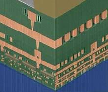
IBM has come up with a technique for using self-assembly to make ultrasmall features in computer chips. The process uses self-assembly to create air gaps as insulation between wires in microprocessors; early tests demonstrate a 35% increase in chip speed and a 15% decrease in power consumption as a result of this technique.
The new self-assembly approach ushers in to chip making an era of nanotechnology, says Daniel Edelstein, IBM fellow and chief scientist for the self-assembly air-gap project. Importantly, Edelstein says, IBM's process is designed to be compatible with current manufacturing facilities and materials.The new process is slated to be implemented in chip manufacturing by 2009. (Somehow I think Moore's Law will be safe for a while yet.)
One of the bottlenecks in the development of today's chips is the copper wiring that passes data between transistors and out of the chip. As chips shrink, these wires, which are about 70 nanometers wide, need to be fabricated closer together. However, the closer the wires are to each other, the more likely their electrical currents are to interfere with each other, sapping energy and slowing data flow. Insulation can help, but today's insulating material--glass--won't be good enough for future generations of chips. Engineers know that air is a better insulator, and they have been working to develop ways to create air gaps small enough--about 35 nanometers in diameter--to work. But the current state-of-the-art manufacturing equipment can't reliably produce air gaps that small.
So instead, IBM researchers used a new type of polymer to help them create the air gaps. The polymer is poured onto copper wires that are embedded in an insulating material. When the polymer is heated, the molecules pull away from each other to form a regular array of nanoscale holes. These holes are used as a template to etch hollow columns into the insulating material that surrounds the wires. Engineers then pump plasma, an electrically charged gas, through the holes to blast away the remaining insulating material. A quick chemical rinse leaves behind clear gaps of air on either side of the copper wires.
If you enjoyed this post, take a few seconds of your time to subscribe to our RSS feed. Barry's Best is updated daily.


0 comments :
Post a Comment